Research and Technical Solutions (RTS)
EXCIMER LASER PHOTOABLATION
What is Photoablation?
Laser photoablation is a highly efficient and versatile etching process by which selected regions in a polymer layer can be removed by high-energy UV laser irradiation. The material is removed in a one-step process, requiring no developing or other steps before or after exposure. In addition to a wide variety of polymeric materials, photoablation has also been succeessfully used for laser-etching of several metals, oxides and other inorganic materials. The largest applications of photoablation include drilling of vias in multilayer microelectronic circuits, fabrication of nozzles in inkjet printheads, and corneal shaping for vision surgery. Numerous other applications of ablation have been implemented and many others are being researched in a variety of electronic, optoelectronic and medical fields.
Photoablation Systems
Laser photoablation can be carried out either in a spot-by-spot fashion using a focused beam from a low-power laser and raster-scanning it to address all the locations, or by projection-imaging the desired pattern of vias, lines, etc. from a mask onto the substrate using a high-power laser, thereby ablating thousands of features simultaneously. In the first case (the serial method), usually an infra-red Nd:YAG laser, frequency-multiplied to either 355 or 266 nm, is used. In the mask-projection technique (the massively parallel method), a high-power UV excimer laser at 351, 308, 248 or 193 nm is used. All of Anvik's production photoablation systems (e.g., HexScan 2150 SXE and HexScan 2100 SPE) are designed for large-area, high-throughput generation of vias and other features using projection imaging, and therefore employ a high-power excimer laser as the light source at one or the other of the above wavelengths.
What Does Anvik RTS Offer?
Beginning with the customer's overall program objectives, the Anvik RTS Division conducts research and development projects of various scopes and durations in photoablation studies. Examples of different types of investigations and feasibility studies we carry out include:
- Characterization of photoablation parameters for a variety of materials important in electronics, optoelectronics, medicine and biotechnology. The parameters that can be investigated include ablation threshold, ablation etch rate, dependence on excimer laser wavelength, and optimum processing conditions. Some examples of materials that can be characterized include polymers, metals, oxides and nitrides, and tissue and other biological materials. Examples of vias, windows and lines ablated in polyimide are shown in Figs. 1 and 2 below.
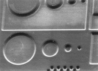
Fig. 1. Photoablated vias and windows.
|

|
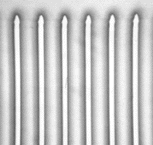
Fig.2. Photoablated trenches.
|
The ablation results shown above were obtained on an Anvik HexScan large-area projection ablation tool that uses a high-power XeCl excimer laser emitting 150 W at 308 nm. Figure 1 shows high-quality vias of 100, 50, 20, and 10 µm diameters ablated in an 8.3-micron-thick film of DuPont Pyralin PI2611 polyimide. The upper part of Fig. 1 shows a large window ablated in the polyimide film, with round pillars left standing within. Figure 2 shows 8-µm-wide lines (trenches) ablated in a 5.6-µm-thick film of the same material.
- Investigation of new materials for their suitability as candidates for processing by photoablation. As advances in new devices, techniques and integrated structures continue to highlight the importance of new materials technologies, processes such as photoablation will continue to have a large impact on the development and characterization of novel materials. Anvik RTS will assist you in investigating such materials.
- Development of a complete turn-key process and equipment proposal for fabrication of the customer's devices, structures or modules. Such a project undertaken by Anvik RTS will deliver a complete manufacturing solution to the customer's manufacturing needs. Systems proposed in such projects may be small modifications of Anvik's core HexScan Series tools, or they may be significantly new configurations should the customer's process, materials and production requirements so dictate.

The other R&D capabilities offered by the Anvik Research and Technical Solutions Division are described in detail in the following sections:
Microlithography
Laser Materials Processing
Optomechanical Systems and Components
Equipment and Facilities
|