|
Ideal as a dual-use (lithography and via-generation) system
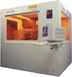
The Anvik HexScanTM 2150 SXE patterning system represents a revolutionary advance in large-format lithography and via-generation systems. It offers the unique combination of high-resolution projection imaging and large-area substrate handling, making it the ideal patterning tool for high-volume, cost-effective production of microelecronic modules and printed circuits. With its excimer laser source emitting 50 watts of UV radiation, this low-cost system serves both as a volume-production resist lithography tool, and as a high-speed, batch via-generation system for dielectric layers.
|
|
|
Large-format substrate handling

|
|
- Designed for projection patterning of substrate sizes of 460 x 610 mm (18 x 24 inches) and larger (1100 x 1250 mm); scalable to 1500 x 1800 mm.
- Capable of handling substrates of a wide range of thicknesses
- Fully automated handling and mask-substrate alignment minimizes overhead time
|
|
High resolution
|
|
- Resolution of 15 microns (0.6 mil) (lines, spaces, holes)
- Patented seamless scanning technology (HexScanTM) delivers lens resolution over entire panel
- High resolution enables excellent line-edge definition and via profiles
|
|
Very high exposure throughput
|
|
Exposure throughputs as high as 180 panels/hr (12 x 12 inch panels), made possible by
- Seamless scanning with hexagonal illumination
- High-power excimer laser illumination system
- High-speed, high-precision scanning stage
|
|
Versatility
|
|
- Delivers very high throughput for lithography in a wide range of photoresist materials
- Capable of high-speed, batch via generation in a variety of polymeric dielectrics
- Available with Anvik's patented Variable-Area Substrate Tiling (VASTTM) technology
|
|
Modularity and upgradability
|
|
- Modular design enables user to define optimum system configuration
- Customer may specify resolution, substrate size parameters and exposure wavelength
- Upgradability of key subsystems extends system life over multiple product generations
|
|
HexScanTM 2150 SXE Specifications
|
|
| Imaging Technique |
Seamless scanning projection |
| Resolution |
15 microns (0.6 mil) |
| Projection System |
1:1 magnification refractive lens |
| Depth of Focus |
1.3 mm (50 mils) |
| Substrate Size |
Up to 1100 x 1250 mm (44 x 50 in), with or without tiling |
| Illumination Source |
XeF excimer laser (other sources optional) |
| Exposure Wavelength |
351 nm (other wavelengths optional) |
| Overlay Precision |
3 microns |
| Alignment System |
Automatic |
| Panel and Mask Handling |
Automatic |
| Exposure Throughput |
>160 panels/hr (12 x 12 in panels) |
| System Price |
USD 800K - 1.3M |
|
For additional information:
- K. Jain et al., "Large-Area, High-Resolution Lithography and Photoablation Systems for Microelectronics and Optoelectronics Fabrication", Proc. IEEE, Vol. 90, No. 10, p. 1681, Oct. 2002. [Click here for a pdf copy of this paper.]
- K. Jain et al., "Large-Area Excimer Laser Lithography and Photoablation Systems", Microlithography World, Vol. 11, No. 3, p. 8, Aug. 2002. [Click here for a pdf copy of this paper.]
- M. Klosner et al., "High-Resolution, Large-Area Projection Lithography Offers a New Alternative for Wafer-Level Packaging", Chip Scale Review, Vol. 6, No. 4, p. 75, Jul. 2002. [On the web: www.ChipScaleReview.com]
- K. Jain et al., "Large-Area, High-Throughput, High-Resolution Lithography Systems for Flat-Panel Displays and Microelectronic Modules," Proc. SPIE, Vol. 3331, p. 197, 1998.
- K. Jain, Large-Area, High-Throughput, High-Resolution Projection Imaging System, U.S. Pat. 5,285,236, issued Feb. 8, 1994.
- K. Jain, Scan and Repeat High Resolution Lithography System, U.S. Pat. 4,924,257, issued May 8, 1990.
|
|