|
Laser projection imaging (LPI) for high-volume production
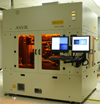
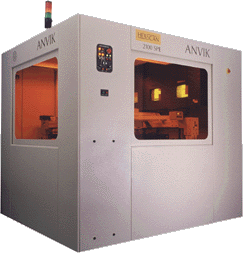
The Anvik HexScanTM 2100 SPE laser projection imaging (LPI) system represents a revolutionary advance in large-format lithography systems. It offers the unique combination of high-resolution projection imaging, large-area substrate handling, and high-precision alignment, making it the ideal exposure tool for cost-effective, volume manufacturing of high-performance printed circuit boards. With its excimer laser illumination source emitting 40 - 50 watts of UV radiation, this high-throughput system serves both as a primary imaging tool for conventional dry-film or liquid resists, and as an efficient exposure system for solder masks and other layers requiring high doses.
|
|
|
Large-format substrate handling

|
|
- Designed for projection imaging of board sizes up to 610 x 915 mm (24 x 36 inches) and larger (1100 x 1250 mm); scalable to 1500 x 1800 mm.
- Capable of handling panels of a wide range of thicknesses, with no mask-to-panel contact
- Ideal for imaging rigid and flexible substrates, and both inner and outer layers
|
|
High resolution, fine alignment
|
|
- Resolution of 10 micron (0.4 mil) features (lines, spaces, holes)
- Patented seamless scanning technology (HexScanTM) delivers lens resolution over entire panel
- Fully automatic alignment with precision of + 2.5 microns (+ 0.1 mil) for layer-to-layer, front-to-back, or mask-to-board registration
|
|
Very high exposure throughput
|
|
Exposure throughputs of 120 panels/hr (18 x 24 inch panels) with conventional photoresists, made possible by
- Seamless scanning with large-area hexagonal illumination beam
- High-power excimer laser illumination system
- Single-planar, high-speed, high-precision scanning stage
|
|
Versatility
|
|
- Delivers very high throughput for lithography in a wide range of photoresist materials
- Capable of patterning with a variety of mask materials, including mylar, glass, and fused silica
- Capable of batch via generation in a variety of polymeric dielectrics
|
|
Modularity and upgradability
|
|
- Modular design enables user to define optimum system configuration
- Available with Anvik's patented independent x-y scaling capability (up to 5000 ppm) to compensate for process-induced dimensional changes in panel (see ref. 3 below)
- Available with Anvik's patented Variable-Area Substrate Tiling (VASTTM) technology to populate panel with modules of different sizes
|
|
HexScanTM 2100 SPE Specifications
|
|
| Imaging Technique |
Seamless scanning projection |
| Resolution |
10 microns (0.4 mil) |
| Projection System |
1:1 magnification refractive lens |
| Depth of Focus |
560 microns (22 mils) |
| Substrate Size |
Up to 1100 x 1250 mm (44 x 50 in), with or without tiling |
| Illumination Source |
XeF excimer laser (other sources optional) |
| Exposure Wavelength |
351 nm (other wavelengths optional) |
| Overlay Precision |
2.5 microns (0.1 mil) |
| Alignment System |
Automatic |
| Panel and Mask Handling |
Automatic |
| Exposure Throughput |
120 panels/hr (18 x 24 in panels) |
| System Price |
USD 750K - 1.2M |
|
For additional information:
- K. Jain et al., "High-Speed, High-Resolution, Large-Area Exposure System for PCB Patterning," Printed Circuit Fabrication, Vol. 20, No. 5, p. 34, May 1997.
- K. Jain et al., "Large-Area, High-Resolution Lithography and Photoablation Systems for Microelectronics and Optoelectronics Fabrication", Proc. IEEE, Vol. 90, No. 10, p. 1681, Oct. 2002. [Click here for a pdf copy of this paper.]
- M. Zemel et al., "X-Y Scaling Compensation Technology for Fine-Line PCB Imaging with High-Precision Alignment", IPC Printed Circuit Expo, Proc. of Technical Conf., p. S03-1-1, Long Beach, CA, Mar. 26-28, 2002. [Click here for a pdf copy of this paper.]
- K. Jain et al., "Large-Area, High-Throughput, High-Resolution Lithography Systems for Flat-Panel Displays and Microelectronic Modules," Proc. SPIE, Vol. 3331, p. 197, 1998.
- K. Jain, Large-Area, High-Throughput, High-Resolution Projection Imaging System, U.S. Pat. 5,285,236, issued Feb. 8, 1994.
- K. Jain, Scan and Repeat High Resolution Lithography System, U.S. Pat. 4,924,257, issued May 8, 1990.
|
|