Research and Technical Solutions (RTS)
EQUIPMENT AND FACILITIES
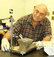
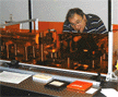
A key element in the strength of Anvik's RTS Division is our extensive resources in equipment and facilities to carry out a wide variety of projects in microelectronic process technologies, electronic and optoelectronic materials, and optomechanical systems and components. Our infrastructure consists of fully operational systems and workstations for lithography, photoablation and materials processing; well-equipped laboratories for optics, electronics and microelectronic processing; state-of-the-art equipment for inspection, test and measurement; and powerful software design tools for optical engineering and mechanical design. Whether your requirements call for feasibility demonstraion of a new process, investigation of a new material, design and construction of a custom optomechanical system, or pilot production run of a new device, our resources enable us to deliver a cost-effective solution for all your research and prototyping needs.
The major resources in equipment and facilities of the Anvik RTS Division are highlighted below.
1. Lithography and Photoablation Systems
- High-resolution, large-area lithography system
- 1 µm resolution on substrate sizes up to 200 x 250 mm
- Capable of patterning on both rigid and flexible substrates
- 248 nm excimer laser projection lithography system
- Large-area lithography system with scaling capability
- 10 µm resolution on substrate sizes up to 350 x 350 mm
- Capable of patterning on both rigid and flexible substrates
- Independent x-y image scaling to compensate for substrate dimensional changes
- 351 nm excimer laser projection lithography system, fully compatible with all i-line photoresists (dry-film and liquid, thin- and thick-film, primary and solder-mask)
- High-resolution photoablation and materials-processing workstation
- Projection system with 5 µm resolution over 30 mm diameter field size
- High-power industrial excimer laser source at 308 nm
- Capable of delivering fluences up to 3 J/cm2
- Ideal for process investigations with polymers, metals, semiconductors, dielectrics and biophotonic materials
2. Industrial Lasers and Other Light Sources
- Lambda Physik high-power XeCl excimer laser at 308 nm
- Lambda Physik high-power KrF excimer laser at 248 nm
- Lambda Physik line-narrowed KrF excimer lasers at 248 nm
- Coherent high-power Argon-ion laser with multiple wavelengths from 351 to 529 nm
- Frequency-doubled Ti:Sapphire laser, tunable from 410 to 460 nm
- High-power, frequency-doubled Nd:YLF laser at 527 nm
- Frequency-stabilized Nd:YAG ring lasers at 1064 nm
- Frequency-quadrupled Nd:YAG laser at 266 nm
- High-power mercury-xenon arc lamp illumination system with multiple wavelengths from 254 to 436 nm
3. Metrology Equipment
Anvik's RTS activities are supported by a wide array of state-of-the-art metrology equipment. In each R&D project carried out by Anvik RTS, we offer complete capabilities to meet all associated test, measurement and evaluation requirements of the project. Our metrology capabilities, listed below, include analysis, measurement and recording of lithography and photoablation results; surface profiling and film thickness measurement; and interferometric testing of high-precision optomechanical assemblies to achieve tight tolerances.
- Hewlett-Packard laser interferometers
- Zygo interferometer system
- Scanning electron and optical microscopes
- High-precision, large-travel air-bearing stages
- Dektak surface profilometer
- Optical spectrum analysis systems
- Multi-element lens centration equipment
- A wide variety of sensors for diverse applications, including Keyence confocal distance sensor and surface profilometer, high-resolution quadrant sensor, CCD cameras and associated imaging optics, HeNe and other alignment lasers, photomultipliers and photodetectors, vibration sensors, etc.
4. Software Design Tools
- Optical design and analysis software
- Mechanical design software
- SolidWorks
- COSMOS
- AutoCAD
5. Processing Facilities
- Cleanroom facility with full environmental controls
- Wet and dry (VLF) process hoods
- Photoresist processing equipment for liquid resists
- Photoresist processing equipment for dry-film resists
- Large-area, photoresist laminating equipment
- Large-area, photoresist spray-developing equipment
- Plasma etching equipment
- Ovens and other miscellaneous processing equipment

The R&D capabilities offered by the Anvik Research and Technical Solutions Division are described in detail in the following sections:
 Excimer Laser Photoablation
Microlithography
Laser Materials Processing
Optomechanical Systems and Components
|