Research and Technical Solutions (RTS)
MICROLITHOGRAPHY
With our diverse expertise in all aspects of lithographic processing, equipment and materials, the Anvik RTS Division provides a complete capability to investigate the requirements of lithographic patterning for any application in microelectronics, optoelectronics, MEMS and biotechnology. Whether your application requires thin-film or thick-film photoresist, i-line or deep UV exposure, rigid or flexible substrate, we can conduct the desired R&D study, assist you with fabricating prototype structures, and develop the optimum solution for your lithographic requirements.
Patterning in Various Photoresists
Depending on the cutomer's design rules, materials compatibilty criteria and product application, our team of lithography professionals conducts patterning investigations in a wide variety of resists, including i-line resists for microelectronics and display fabrication; thick-film resists for MEMS, optoelectronics and wafer-level applications; dry-film, liquid and solder-mask resists for printed circuits, microvia and other HDI products; and deep UV-resists for high-resolution applications.
Imaging with Different Wavelengths
Anvik's RTS laboratories are equipped with several lithography exposure stations that use excimer lasers of different wavelengths. Our lithography tools that incorporate a XeF laser emitting at 351 nm are ideal for investigations that require patterning in i-line photoresists. For deep UV applications, Anvik offers exposure tools that incorporate a KrF excimer laser operating at 248 nm. In addition, our facilities also include exposure stations employing 308 nm XeCl lasers -- this wavelength is ideal when the project objectives require the capabilities of both conventional lithography (i.e., expose and wet-develop) and photoablation, as offered by, for example, the Anvik HexScan 2150 SXE system. Such a dual capability is highly attactive for a variety of fabrication processes and materials.
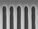
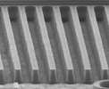
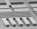
Three examples of lithographic imaging results obtained with Anvik's projection lithography systems are shown below in Figs. 3-5. Several additional examples are presented at the link Demonstrated Results.
The 1 µm images shown in Fig. 3 were obtained on an Anvik HexScan 1010 SDE deep-UV projection lithography tool that uses a 248-nm KrF excimer laser. Figure 4 shows 10 µm lines and spaces patterned in a 13-µm-thick liquid resist using an Anvik HexScan 2100 SPE system designed for fine-line PCB imaging; patterns imaged in a conventional dry-film PCB resist using the same tool are shown in Fig. 5.
Patterning on Different Types of Substrates
Since Anvik develops and builds lithography systems for a variety of products, including microelectronics, displays, optoelectronics, MEMS, printed circuits and flexible electronics, we have extensive experience and resources in lithographic patterning on a wide range of substrate materials. Whether your application requires glass plates or silicon wafers, polymer sheets or ceramic layers, rigid or flexible panels, we invite you to contact us to assist you with planning and carrying out the desired lithographic R&D investigation.

The other R&D capabilities offered by the Anvik Research and Technical Solutions Division are described in detail in the following sections:
 Excimer Laser Photoablation
Laser Materials Processing
Optomechanical Systems and Components
Equipment and Facilities
|