Demonstrated Performance
The excellent performance of the Anvik laser projection patterning systems has been demonstrated for both fine-line lithographic imaging in photoresists, and high-speed, batch via generation by ablation in polymeric dielectrics.
Examples presented here are of high-quality lithographic patterning in various conventional photoresists (Figures 1-6) and of high-quality, mask-projection ablation of vias and lines in a commonly used polymer (Figures 7-9).
The results shown in Figures 1 -4 were obtained on an Anvik laser projection imaging system designed for high-throughput, high-resolution patterning for volume production of fine-line printed circuits on rigid and flexible panels. This system, the HexScanTM 2100 SPE, uses a 0.025 NA projection lens and a 351 nm XeF excimer laser illumination source, and has a resolution capability of 10 microns (0.4 mil).
The results shown in Figures 5-9 were obtained on an Anvik HexScanTM 3030 SXE patterning system designed for high-resolution imaging, photoablation and laser crystallization for production of displays, optoelectronic devices, microelectromechanical sysems (MEMS), and multi-chip modules. This system uses a 0.07 NA projection lens and a 308 nm XeCl excimer laser illumination source, giving a resolution capability of 3 microns.
The SEM image shown in Figure 10 is of an exposure made on an Anvik deep-UV laser projection imaging system designed for high-resolution, high-throughput patterning for volume production of displays, microelecronics, and optoelectronic devices. This system, the HexScanTM 1010 SDE, uses a 0.18 NA projection lens and a 248 nm KrF excimer laser illumination source, and has a resolution capability of 1 micron.
Figures 1 & 2. Laser projection imaging for fine-line PCB production. A variety of commercial dry-film photoresists, applied on 18 x 24 inch laminate PCB boards, were imaged on the Anvik HexScanTM 2100 SPE system using conventional mylar masks. Figure 1 shows 50 micron(2 mil)-wide lines and spaces patterned in 30 micron(1.2 mil)-thick photoresist. Figure 2 presents 36 micron (1.4 mil)-wide lines and spaces obtained in the same exposure.
Figures 3 & 4. Laser projection imaging for fine-line PCB production. Exposues made on the Anvik HexScanTM 2100 SPE system in a commercial liquid photoresist using a conventional chrome-on-glass mask. Figure 3 (top) shows 20 micron(0.8 mil)-wide lines and spaces patterned in 13 micron(0.5 mil)-thick photoresist. Figure 4 (bottom) presents 10 micron (0.4 mil)-wide lines and spaces obtained in the same exposure.
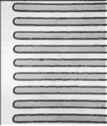
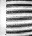
Figures 5 & 6. High-resolution lithography results. A variety of commercial thin-film photoresists, applied on glass plates or Si wafers, were imaged on the Anvik HexScanTM 3030 SXE using various fused silica masks. Figure 5 (left) shows 5 micron-wide lines and spaces patterned in 1.1 micron-thick UCB-JSR080TI photoresist. Figure 6 (right) presents 3 micron-wide lines and spaces obtained in the same exposure.
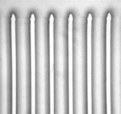
Fig. 9
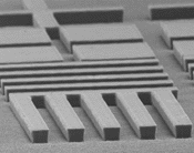
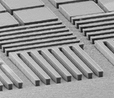
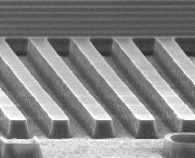
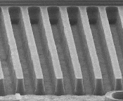
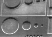
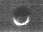
Figures 7-9. Photo-ablation results: Vias, windows, and lines. A variety of polyimides, used in various thicknesses spun on fused silica plates or as free-standing films, were ablated on the Anvik HexScanTM 3030 SXE using a dielectric mask. Figure 7 (top) shows high-quality vias of 100, 50, 20, and 10 micron diameters ablated in an 8.3 micron-thick film of DuPont Pyralin PI2611 spun on a fused silica plate. The upper part of Fig. 7 shows a large window ablated in the polyimide film, with round pillars left standing within. Figure 8 (middle) presents an enlarged view of the 20-micron via. Note the tapered wall profile, which is attractive for metal plating when the via is formed in an interlayer dielectric in HDI products. Figure 9 (bottom) shows 8 micron-wide lines (trenches) ablated in a 5.6 micron-thick film of the same material.
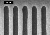
Figure 10. Large-area, 1-µm imaging for displays, microelectronics, and optoelectronic devices. Scanning electron micrograph showing 1 µm lines and spaces patterned with the Anvik HexScan TM 1010 SDE high-resolution, large-area microlithography system in 1 µm thick deep UV photoresist.

|