|
Breakthrough Performance
Novel, Large-Area, High-Resolution, High-Throughput Lithography and Via Generation System Technology
In the detailed description below, we present Anvik's scanning projection technology for high-volume manufacturing. In addition to a family of such scanning systems (HexScan), Anvik also offers a low-cost step-and-repeat system (NexStep) that is ideal for prototyping as well as carrying out R&D in lithography and laser ablation applications.
In the manufacturing of numerous electronic products, such as microelectronic modules, flat-panel displays (FPDs), communication electronics, microelectromechanical systems (MEMS), printed circuit boards (PCBs), and flexible circuits, it is necessary to fabricate millions of microscopic structures on a single large substrate. One of the most critical equipment requirements in these applications is a large-area patterning system that can provide the required resolution over the entire substrate with high processing throughput. Anvik Corporation has developed a class of novel projection patterning systems whose performance exceeds such demanding requirements. No other exposure systems currently exist that meet all the desired performance criteria satisfactorily.
The Anvik scanning exposure systems provide both high-throughput resist lithography and dielectric photoetching for production of large-format electronic modules on rigid as well as flexible substrates. The proven technology combines high resolution with large-area imaging capability, eliminating the limitations of other lithography tools, including contact and proximity tools, conventional projection systems, steppers and scanners, and direct-write machines. Further, the Anvik systems are highly modular, providing equipment upgradability as well as choice of user-specified system configurations. These features are achieved with a novel seamless scanning technique and opto-mechanical system configurations that provide both high optical and scanning efficiencies, delivering lithography throughputs as high as 6 sq. ft./min and via generation speeds of several tens of thousandsof vias/sec. Anvik now offers production systems with lithographic resolution ranging from 25 microns (0.001 inch) to less than 1 micron (0.00004 inch) and via-etching capability from 100 micron (0.004 inch) down to 10 micron (0.0004 inch) diameter vias, deliverable on discrete substrates of sizes up to 44 x 50 inches (1100 x 1250 mm), as well as on roll-fed flexible substrates of various widths. The technology is readily scalable to panel sizes of 60 x 72 inches (1500 x 1800 mm).
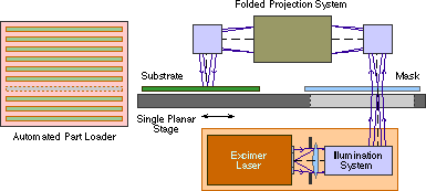
Figure 1. A schematic illustration of Anvik's large-area, high-resolution, high-throughput, projection patterning system technology. The figure shows, in side view, a substrate and a mask held rigidly on a single planar x-y scanning stage, an illumination system having an excimer laser light source, a projection lens assembly, a reversing unit, and an automated substrate loader.
Anvik's new patterning system technology (1-5) is illustrated in Fig. 1 (above) and Fig. 2 (below). The substrate and mask are mounted on a single planar stage which is capable of moving in both x- and y-directions. The illumination system has an emission plane in the shape of a hexagon, which is imaged by a condenser at the mask. A 1:1 projection lens images the illuminated hexagonal pattern on the mask on to the substrate. The single planar stage causes the mask and the substrate to scan in unison along the x-axis across their respective illumination regions to traverse the substrate length. The stage then moves along y by an effective scan width (w in Fig. 3). Now the substrate and mask are again scanned along x as before, after which they are laterally moved along y, and the process is repeated until the entire substrate is exposed. The complementary overlap between adjacent hexagonal scans produces a totally seamless and uniform exposure on the whole substrate.
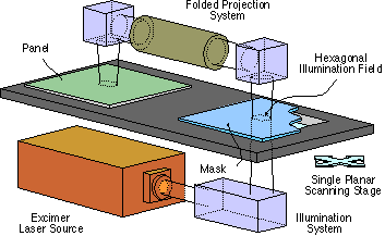
Figure 2. A perspective illustration of the Anvik large-area patterning system shown before as a side-view schematic in Fig. 1. Note the hexagonal illumination region on the mask, which is imaged by the projection system on to the corresponding location on the substrate.
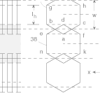
Figure 3 (below) illustrates the seamless scanning mechanism in more detail. The regular hexagons 36 and 38 represent the illuminated regions on the substrate for scans 1 and 2. The y-movement of the substrate after each x-scan is given by w = 1.5 lh, where lh is the length of each side of the hexagon. In scan 1, the region swept by the rectangular portion b-g-h-c of hexagon 36 is not overlapped by any portion of scan 2. However, the region swept by the triangular segment a-b-c of hexagon 36 in scan 1 is re-swept in scan 2 by the triangular segment d-e-f of hexagon 38. When the doses from these triangular segments are integrated, the cumulative exposure dose anywhere in the overlapping region is the same as in the non-overlapping regions, thus producing a seamless, uniform exposure over the whole substrate.
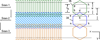
Figure 3. The hexagonal seamless scan-and-repeat exposure mechanism, showing three successive scans and complementary exposure in the partial overlap areas between adjacent hexagonal scanning regions, which results in seamless and uniform imaging over the whole substrate.
The seamlessness of the cumulative dose received by the substrate is further clarified with the help of Fig. 4 (below). Since the exposure in each scan is carried out with an illumination beam of hexagonal cross-section, the integrated dose delivered by each scan has a trapezoidal profile in the lateral (y) direction. The partial overlap between adjacent trapezoidal profiles is so arranged that they intersect at the mid-point of their tapering sections. As shown in Fig. 4, this results in a cumulative dose profile from all scans that is totally seamless. In other words, the exposure of the entire substrate is completely free of stitching errors.
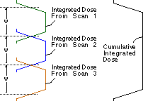
Figure 4. Seamless joining of hexagonal scans. The profile of the energy dose delivered to the substrate in each hexagonal scan is trapezoidal; overlap between tapering sections of adjacent scan profiles produces seamless and uniform cumulative exposure.
Thus, the Anvik system approach makes it possible to obtain the desired resolution by selecting a projection lens of a suitable numerical aperture, and deliver that resolution over very large substrate areas efficiently by the technique of hexagonal seamless scanning. Note also that, since the mask and substrate are mounted rigidly on a single planar stage, issues concerning relative mask-substrate movements during imaging are eliminated. Another key advantage of the Anvik system that is significant with respect to cost-of-ownership comparisons is its elegant, modular design -- the main subsystems, including the illumination module, the imaging module and the stage module, are integrated in a mutually non-interfering manner. This important and unique feature permits not only choice of different user-specified system configurations, but also future upgradability of the system as products migrate from one generation to the next. The Anvik system is the cost-effective solution for large-area, high-resolution lithography and via generation.
For additional information:
- K. Jain et al., "Large-Area, High-Resolution Lithography and Photoablation Systems for Microelectronics and Optoelectronics Fabrication", Proc. IEEE, Vol. 90, No. 10, p. 1681, Oct. 2002. [Click here for a pdf copy of this paper.]
- K. Jain et al., "Flexible Electronics and Displays: High-Resolution, Roll-to-Roll, Projection Lithography and Photoablation Processing Technologies for High-Throughput Production", Proc. IEEE, Vol. 93, No. 8, p. 1500, Aug. 2005. [Click here for a pdf copy of this article.]
- "New Patterning Technology Makes Faster Electronics, Sharper Displays," BMDO Update (U.S. Dept. of Defense, Ballistic Missile Defense Organization, Newsletter of the Technology Applications Program), Issue No. 37, Spring 2001, p. 8. [Click here for a pdf copy of this article.]
- K. Jain et al., "Large-Area Excimer Laser Lithography and Photoablation Systems", Microlithography World, Vol. 11, No. 3, p. 8, Aug. 2002. [Click here for a pdf copy of this paper.]
- M. Klosner et al., "High-Resolution, Large-Area Projection Lithography Offers a New Alternative for Wafer-Level Packaging", Chip Scale Review, Vol. 6, No. 4, p. 75, Jul. 2002. [See also: www.ChipScaleReview.com]
- K. Jain, Large-Area, High-Throughput, High-Resolution Projection Imaging System, U.S. Pat. 5,285,236, issued Feb. 8, 1994.
|