|
Ideal low-cost mini-stepper for lithography and photoablation R&D and prototyping
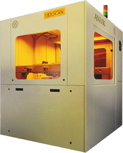
The Anvik NexStepTM 1020 SXE microlithography system is a revolutionary advance in multifunction laser processing systems. It is a low-cost step-and repeat tool designed for R&D and prototyping. It offers the unique combination of high-resolution projection lithography in photoresists, photoablation in polymers, and high-fluence materials processing of semiconductors and other materials, making it the ideal patterning tool for prototyping and pilot production as well as exploration of new frontiers in micro-optics, optoelectronics, MEMS, microfluidics, and biophotonics in a multi-user, multidisciplinary environment.
|
|
|
High resolution projection imaging

|
|
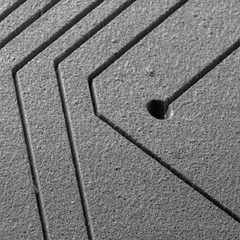
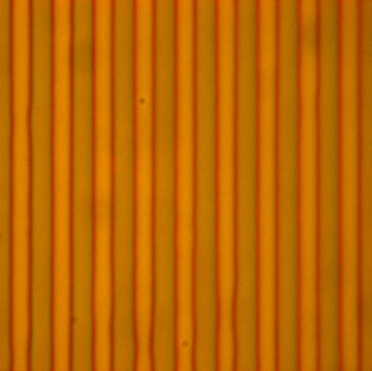
- Diffraction-limited projection system provides optical resolution of 2 microns over entire field
- High resolution produces channels, holes, etc. with excellent edge definition and wall profiles
- Projection imaging eliminates limitations of contact / proximity printing and direct writing
|
|
Versatile Substrate Handling
|
|
- Designed for processing substrates of different sizes and shapes (up to 150 x 150 mm or 150 mm dia.)
- Capable of patterning on substrates of a wide range of thicknesses - from 0.5 to 5.0 mm
- Able to handle both rigid (Si wafers, glass plates, etc.) and flexible (e.g., polymer sheets) materials
|
|
Multifunction capability
|
|
- High-resolution projection patterning of photoresists, polymers and biosurfaces
- Fabrication of MEMS, integrated optics and microfluidics in rigid and flexible materials
- Laser crystallization of amorphous semiconductors and optoelectronic films for displays and integrated sensors
|
|
Versatility and upgradability
|
|
- Ideal for process development and materials investigations for diverse applications
- Upgradable to higher resolutions (submicron) and larger substrate sizes (> 1000 cm2)
- Readily optimized for dedicated use with any specific process and / or materials set
|
|
Technology transfer vehicle
|
|
- System is ideal 'pilot tool' for technology transfer to high-volume manufacturing
- Projection system and excimer laser source deliver high resolution, yield and throughput
- Upgrade to seamless scanning system enables rapid transition to large-format processing
|
|
NexStepTM 1020 SXE Specifications
|
|
| Imaging Technique |
Projection step-and-repeat |
| Resolution |
2 microns (0.08 mil) for photolithography and 5 microns (0.2 mil) for photoablation |
| Projection System |
5:1 reduction refractive lens |
| Depth of Focus |
14 microns (0.56 mil) for 2 micron resolution; 35 microns (1.4 mils) for 5 micron resolution |
| Substrate Size |
Up to 150 x 150 mm (6 x 6 in) or 150 mm dia. |
| Substrate Thickness |
0.05 mm (2 mils) to 5 mm |
| Illumination Source |
XeCl excimer laser (KrF or XeF optional) |
| Exposure Wavelength |
308 nm (248 or 351 nm optional) |
| Fluence at Substrate |
Up to 1 J/cm2 |
| Substrate Handling |
Manual |
| Alignment System |
Manual (automatic optional) |
| System Price |
USD 350 - 400K |
|
|