|
Ideal for lithography on large panels
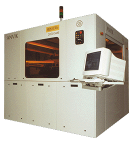
The Anvik HexScanTM 2050 SME patterning system represents a revolutionary advance in large-panel microlithography systems. It offers the attractive combination of high-resolution projection imaging and large-area substrate handling, making it the ideal patterning tool for high-volume, cost-effective production of high-density microelectronic modules, opto-electronic devices, communication electronics, and displays. With its unique variable-area substrate tiling (VASTTM) technology, which enables processing of different multiple-up module configurations, this low-cost system serves both as a volume-production lithography system, and as a versatile development tool for prototyping a wide range of microelectronic and optoelectronic devices.
|
|
|
Large-format substrate handling

|
|
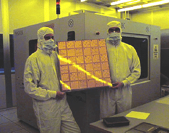
- Designed for projection patterning on panel sizes of 610 x 610 mm (24 x 24 inches) and larger (1100 x 1250 mm); scalable to 1500 x 1800 mm.
- Capable of handling substrates of a wide range of thicknesses
- Automated mask-substrate alignment and part handling minimizes overhead time
|
|
High resolution
|
|
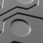
- Resolution of 5 microns (0.2 mil) (lines, spaces, holes)
- High resolution enables excellent line-edge definition and ablation profiles
- Patented seamless scanning technology (HexScanTM) delivers lens resolution over entire panel
|
|
Very high exposure throughput
|
|
Exposure throughputs as high as 180 panels/hr (12 x 12 inch panels), made possible by
- Seamless scanning with hexagonal illumination
- Efficient excimer laser illumination system
- High-speed, high-precision scanning stage

|
|
Versatility
|
|
- Delivers very high throughput for lithography in common resists
- Enables prototyping of different substrates and module sizes for electronic and opto-electronic devices
- Patented Variable-Area Substrate Tiling (VASTTM) technology enables multiple-up substrate configuration
|
|
Modularity and upgradability
|
|
- Modular design enables user to define ideal system configuration
- Customer may specify resolution, substrate type and size parameters, and exposure wavelength
- Upgradability of key subsystems extends system life over multiple product generations
|
|
HexScanTM 2050 SME Specifications
|
|
| Imaging Technique |
Seamless scanning projection |
| Resolution |
5 microns (0.2 mil) |
| Projection System |
1:1 magnification refractive lens |
| Depth of Focus |
140 microns (5.5 mils) |
| Substrate Size |
Up to 1100 x 1250 mm (44 x 50 in), with or without tiling |
| Illumination Source |
XeF excimer laser (other sources optional) |
| Exposure Wavelength |
351 nm (other wavelengths optional) |
| Overlay Precision |
1 micron (0.04 mil) |
| Alignment System |
Automatic |
| Substrate Handling |
Multiple-up module configuration, with variable-area substrate tiling (VASTTM) |
| Exposure Throughput |
>160 panels/hr (12 x 12 in panels) |
| System Price |
USD 950K - 1.4M |
|
For additional information:
- K. Jain et al., "Large-Area, High-Resolution Lithography and Photoablation Systems for Microelectronics and Optoelectronics Fabrication", Proc. IEEE, Vol. 90, No. 10, p. 1681, Oct. 2002. [Click here for a pdf copy of this paper.]
- M. Robertsson et al., "Large-area patterning of high-density interconnects by novel UV-excimer lithography and photo-patternable ORMOCERTM dielectric," presented at the International Microelectronics and Packaging Society (IMAPS) Conference, Strassbourg, France, May 30-June 1, 2001. [Click here for a pdf copy of this paper.]
- K. Jain et al., "Large-Area Excimer Laser Lithography and Photoablation Systems", Microlithography World, Vol. 11, No. 3, p. 8, Aug. 2002. [Click here for a pdf copy of this paper.]
- "New Patterning Technology Makes Faster Electronics, Sharper Displays," BMDO Update (U.S. Dept. of Defense, Ballistic Missile Defense Organization, Newsletter of the Technology Applications Program), Issue No. 37, Spring 2001, p. 8. [Click here for a pdf copy of this article.]
- K. Jain, Large-Area, High-Throughput, High-Resolution Projection Imaging System, U.S. Pat. 5,285,236, issued Feb. 8, 1994.
- T. Dunn, N. Farmiga and K. Jain, Projection Patterning of Large Substrates Using Limited-Travel X-Y stage, U.S. Pat. 5,897,986, issued Apr. 27, 1999.
|
|