|
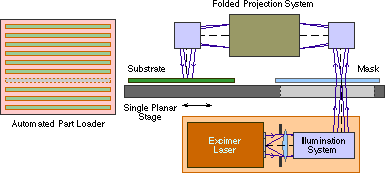
FIGURE 1: A schematic illustration of Anvik's large-area, high-resolution, high-throughput, projection patterning system technology. The substrate and a mask are mounted rigidly on a single planar x-y scanning stage. An illumination system comprising a high-power UV excimer laser and beam conditioning optics illuminates the mask from below in a uniform hexagon-shaped region. The illuminated region on the mask is imaged by the projection system on to the substrate. The projection lens has the required numerical aperture to produce the desired resolution. The reversing unit ensures that the mask pattern and its image on the substrate are in the same orientation. The stage is scanned in such a way that the illumination region traverses across the whole mask. Partial overlapping of complementary exposure dose profiles delivered in adjacent scans produces seamless imaging of the entire substrate, eliminating stitching errors as well as substrate size limitations. The same system technology forms the basis for both projection lithography in photoresists, and high-speed via generation by projection photo-ablation. | ||
| ||
Figure 2: A schematic llustration of the Anvik high-resolution patterning system with VASTTM (Variable-Area Substrtae Tiling) capabiliy. While preserving all the benefits of Anvik's core technology of large-area, seamless projection imaging (Figure 1, above), the VAST technology allows the user, in addition, to pattern modules of different sizes on a single standard substrate. This simplifies the substrate handling issues for all processing steps. With VAST capability, it is possible to perform a single, global alignment of the entire mask and substrate, or perform site-by-site alignment for individual modules. Additionally, the technology allows the user to share the processing of several low-volume products on a high-volume platform. Finally, the VAST technology enables the user to determine mask sizes based on the size of each module, rather than the whole substrate. Decreasing mask size makes the manufacturing process more economical and robust. | ||
|