|
Ideal for patterning on flexible substrates
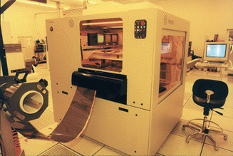
The Anvik HexScanTM 3100 SRE patterning system for flexible substrates represents a revolutionary advance in large-area lithography systems. It offers the unique combination of high-resolution projection imaging and roll-to-roll substrate handling, making it the ideal patterning tool for high-volume, low-cost production of communication electronics, printed circuits, automotive electronics, and displays on flexible materials. With its high-power excimer laser illumination source, the system serves both as a high-throughput lithography tool for photoresist materials, and as a high-speed, batch via generation system for dielectric layers.
|
|
|
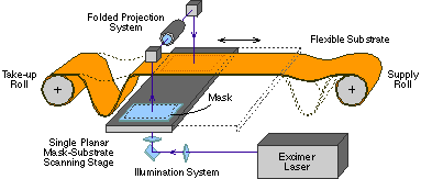
Roll-to-roll substrate handling

|
|
- Designed for projection patterning of flexible, roll-fed substrates of various materials
- Capable of handling rolls of widths 35 to 610 mm (1.4 to 24 inches) and various thicknesses
- Fully automated feed and alignment of print area minimizes overhead time
|
|
High resolution
|
|
- Resolution of 10 microns (0.4 mil) (lines, spaces, holes)
- Patented seamless scanning technology (HexScanTM) delivers lens resolution over entire panel
- High resolution enables excellent line-edge definition and via profiles
|
|
Very high exposure throughput
|
|
Exposure throughputs as high as 6 sq. ft. per minute, made possible by:
- Seamless scanning with hexagonal illumination
- High-power excimer laser illumination system
- High-speed, high-precision scanning stage
|
|
Versatility
|
|
- Delivers very high exposure throughput for lithography in resist materials
- Capable of high-speed, batch via-generation in polymeric dielectricss
- Availability of very high fluence levels allows use of wide range of resists and dielectrics
|
|
Modularity and upgradability
|
|
- Modular design enables user to define optimum system configuration
- Customer may specify resolution, substrate size parameters and exposure wavelength
- Upgradability of key subsystems extends system life over multiple product generations
|
|
HexScanTM 3100 SRE Specifications |
|
| Imaging Technique |
Seamless scanning projection |
| Resolution |
10 microns (0.4 mil) |
| Projection System |
1:1 magnification refractive lens |
| Depth of Focus |
560 microns (22 mils) |
| Width of Substrate Roll |
13.4 inches (other sizes optional) |
| Panel Exposure Area |
12 by 12 inches (other sizes optional) |
| Illumination Source |
XeF excimer laser (other sources optional) |
| Exposure Wavelength |
351 nm (other wavelengths optional) |
| Overlay Precision |
2.5 microns |
| Alignment System |
Automatic |
| Panel and Mask Handling |
Automatic |
| Exposure Throughput |
> 4 sq ft/min [240 panels/hr (12 x 12 inch panels)] |
| System Price |
USD 1.3 - 2.2M |
|
For additional information:
- K. Jain et al., "Flexible Electronics and Displays: High-Resolution, Roll-to-Roll, Projection Lithography and Photoablation Processing Technologies for High-Throughput Production", Proc. IEEE, Vol. 93, No. 8, p. 1500, Aug. 2005. [Click here for a pdf copy of this article.]
- K. Jain et al., "Large-Area, High-Resolution Lithography and Photoablation Systems for Microelectronics and Optoelectronics Fabrication", Proc. IEEE, Vol. 90, No. 10, p. 1681, Oct. 2002. [Click here for a pdf copy of this paper.]
- K. Jain et al., "Large-Area Excimer Laser Lithography and Photoablation Systems", Microlithography World, Vol. 11, No. 3, p. 8, Aug. 2002. [Click here for a pdf copy of this paper.]
- K. Jain et al., "Lithography on Flexible Substrates: A Roll-to-Roll, High-Throughput, High-Resolution System for Low-Cost Production of Microelectronics," Proc. SPIE, Vol. 3331, p. 207, 1998.
- K. Jain, High-Throughput, High-Resolution Projection Patterning System for Large, Flexible, Roll-Fed, Electronic-Module Substrates, U.S. Pat. 5,652,645, issued Jul. 29, 1997.
- K. Jain, Large-Area, High-Throughput, High-Resolution Projection Imaging System, U.S. Pat. 5,285,236, issued Feb. 8, 1994.
|
|