|
Wide-field lithography for high-throughput wafer-level packaging
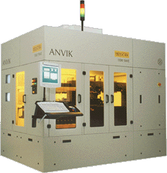
The Anvik HexScanTM 1100 SWE wide-field laser lithography system represents a revolutionary advance in patterning systems for wafer-level packaging applications. It offers the unique combination of high-resolution projection imaging, high-precision alignment, and ability to handle silicon wafers and other substrates up to 300 mm in size, making it the ideal exposure tool for cost-effective, volume manufacturing of wafer-level products and other high-performance electronic packages. With its excimer laser illumination source, seamless imaging over the entire wafer area, and automatic wafer loading and unloading, this high-throughput system eliminates the limitations of other exposure tools such as contact and proximity printers, steppers and direct writers.
|
|
|
Large-format substrate handling

|
|
- Designed for projection imaging of silicon wafers of diameters up to 300 mm and other substrates of sizes up to 300 x 300 mm
- Ideal for handling substrates of a wide range of thicknesses, including very thin wafers (down to 150 �m thickness)
- Capable of exposing large package sizes, addressing the requirements of WLP, SOC, MEMS, and integrated optoelectronic packages
- Capable of imaging rigid and flexible substrates, with no mask-to-substrate contact
- Automatic wafer and mask handling capability
|
|
High resolution, fine alignment
|
|
- Resolution of 10 micron (0.4 mil) features (lines, spaces, holes)
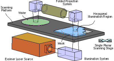
- Patented seamless scanning technology (HexScanTM) delivers specified resolution over entire substrate
- Fully automatic high-speed alignment with precision of + 2.5 microns (+ 0.1 mil) for mask-to-wafer and layer-to-layer registration
|
|
High exposure throughput
|
|
Exposure throughputs of over 100 wafers/hr with conventional photoresists, made possible by
- Seamless scanning with large-area hexagonal illumination beam
- Excimer laser illumination system
- Single-planar, high-speed, high-precision scanning stage
|
|
Versatility
|
|
- Delivers very high throughput for lithography in a wide range of thin and thick photoresist materials
- Capable of patterning with a variety of mask materials, including glass, fused silica and mylar
- Provides large DOF for exposures in thick resists and increased tolerance of non-planar substrates
- Capable of robotic handling of rigid and non-rigid substrates
|
|
Modularity and upgradability
|
|
- Available in resolution capability down to 1 �m
- Robotic interface is customizable to enable handling of substrates of different sizes and shapes
- Available with Anvik's patented independent x-y scaling capability (up to 5000 ppm) to compensate for process-induced dimensional changes in substrate (see Ref. 3 below)
|
|
HexScanTM 1100 SWE Specifications
|
|
| Imaging Technique |
Seamless scanning projection |
| Resolution |
10 microns (0.4 mil) |
| Projection System |
1:1 magnification refractive lens |
| Depth of Focus |
560 microns (22 mils) |
| Substrate Size |
Up to 300 mm dia. or 300 x 300 mm sq. |
| Illumination Source |
XeF excimer laser (other sources optional) |
| Exposure Wavelength |
351 nm (other wavelengths optional) |
| Overlay Precision |
2.5 microns (0.1 mil) |
| Alignment System |
Automatic |
| Wafer and Mask Handling |
Automatic |
| Exposure Throughput |
100 wafers/hr |
| System Price |
USD 750K - 1.2M |
|
For additional information:
- K. Jain et al., "Large-Area, High-Resolution Lithography and Photoablation Systems for Microelectronics and Optoelectronics Fabrication", Proc. IEEE, Vol. 90, No. 10, p. 1681, Oct. 2002. [Click here for a pdf copy of this paper.]
- M. Klosner et al., "High-Resolution, Large-Area Projection Lithography Offers a New Alternative for Wafer-Level Packaging," Chip Scale Review, Vol. 6, No. 4, p. 75, July 2002. [Click here to view full paper.]
- K. Jain et al., "Large-Area Excimer Laser Lithography and Photoablation Systems", Microlithography World, Vol. 11, No. 3, p. 8, Aug. 2002. [Click here for a pdf copy of this paper.]
- K. Jain et al., "Large-Area, High-Throughput, High-Resolution Lithography Systems for Flat-Panel Displays and Microelectronic Modules," Proc. SPIE, Vol. 3331, p. 197, 1998.
- K. Jain, Large-Area, High-Throughput, High-Resolution Projection Imaging System, U.S. Pat. 5,285,236, issued Feb. 8, 1994.
|
|