|
Ideal for micron-level lithography on large substrates
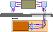
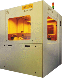
The Anvik HexScanTM 1010 SDE microlithography system represents a revolutionary advance in large-format lithographic patterning systems. It offers the unique combination of high-resolution projection imaging and large-area substrate handling, making it the ideal microlithography tool for high-volume, cost-effective production of high-definition flat-panel displays and other optoelectronic and microelectronic products requiring micron-level patterning.
|
|
|
Large-format substrate handling

|
|
- Designed for projection imaging of substrates of sizes up to 250 x 350 mm (10 x 14 inches)
- Capable of handling substrates of a wide range of thicknesses
- Fully automated handling and mask-substrate alignment minimizes overhead time
|
|
High resolution
|
|
- Resolution of 1 micron (lines, spaces, holes)
- Patented seamless scanning technology (HexScanTM) delivers lens resolution over entire panel
- High resolution produces lines and holes with excellent edge definition and wall profiles
|
|
Very high exposure throughput
|
|
Exposure throughputs as high as 100 panels/hr (10 x 14 inch panels), made possible by
- Seamless scanning with hexagonal illumination
- High-power excimer laser illumination system
- High-speed, high-precision scanning stage
|
|
Versatility
|
|
- Delivers very high throughput for high-resolution lithography in photoresists
- Capable of photoetching various polymeric dielectrics
- Available with Anvik's patented Variable-Area Substrate Tiling (VASTTM) technology
|
|
Modularity and upgradability
|
|
- Modular design enables user to define optimum system configuration
- Customer may specify resolution and substrate size parameters
- Upgradability of key subsystems extends system life over multiple product generations
|
|
HexScanTM 1010 SDE Specifications
|
|
| Imaging Technique |
Seamless scanning projection |
| Resolution |
1 micron |
| Project System |
1:1 magnification refractive lens |
| Depth of Focus |
8 microns |
| Substrate Size |
Up to 250 x 350 mm (10 x 14 in), with or without tiling |
| Illumination Source |
KrF excimer laser (other sources optional) |
| Exposure Wavelength |
248 nm (other wavelengths optional) |
| Overlay Precision |
0.3 micron |
| Alignment System |
Automatic |
| Panel and Mask Handling |
Automatic |
| Exposure Throughput |
> 90 panels/hr (10 x 14 in panels) |
| System Price |
USD 1.4 - 2.0M |
|
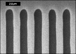
Scanning electron micrograph showing 1 µm lines and spaces patterned with the Anvik HexScan TM 1010 SDE high-resolution, large-area microlithography system in 1 µm thick deep UV photoresist.
For additional information:
- K. Jain et al., "Large-Area, High-Throughput, High-Resolution Lithography Systems for Flat-Panel Displays and Microelectronic Modules," Proc. SPIE, Vol. 3331, p. 197, 1998.
- K. Jain et al., "High-Resolution Laser Projection Imaging for Display Production," in Global Semiconductor Manufacturing Technology, published by World Markets Research Center, London, UK (www.wmrc.com), January 2001.
- "New Patterning Technology Makes Faster Electronics, Sharper Displays," BMDO Update (U.S. Dept. of Defense, Ballistic Missile Defense Organization, Newsletter of the Technology Applications Program), Issue No. 37, Spring 2001, p. 8. [Click here for a pdf copy of this article.]
- K. Jain, "A Novel High-Resolution Large-Field Scan-and-Repeat Projection Lithography System," Proc. SPIE, Vol. 1463, p. 666, 1991.
- K. Jain, Large-Area, High-Throughput, High-Resolution Projection Imaging System, U.S. Pat. 5,285,236, issued Feb. 8, 1994.
- K. Jain, Scan and Repeat High Resolution Lithography System, U.S. Pat. 4,924,257, issued May 8, 1990.
|
|