|
News About Anvik's Upcoming Trade Exhibitions, Recent Press Releases, New Technical Articles, and Recently Announced Products and Services

December 2013
Anvik president Kanti Jain elected Fellow of AAAS

|

|
Washington, DC -- Dr. Kanti Jain, professor of Electrical and Computer Engineering at the University of Illinois at Urbana-Champaign and president of Anvik Corporation, has been elected a Fellow of the American Association for the Advancement of Science. As described by AAAS, fellows are honored for their "scientifically or socially distinguished efforts to advance science or its applications." Dr. Jain was recognized for his "invention and development of fundamental manufacturing processes and systems for high-resolution and large-area micro- and nanolithography." In the early 1980s, he pioneered the laser lithography techniques now commonplace in microchip manufacturing. In the 1990s, he invented the large-area lithography technologies widely used today in the production of flat-screen televisions.
|
Novemebr 2013
Lawsuits filed by Anvik against Nikon and certain of Nikon's customers are settled
New York, NY -- The U.S. patent infringement actions brought by Anvik Corporation against Nikon Corporation, certain of Nikon's affiliates, and certain users of Nikon microlithography machines have been voluntarily discontinued as a result of a settlement under which Nikon made a payment to Anvik and Anvik agreed not to assert its patents-in-suit against Nikon, its affiliates, users of its microlithography machines, or customers of the users of Nikon's microlithography machines.
May 2010
Anvik president Kanti Jain's pioneering development of excimer laser lithography featured in 50 Years of Laser History Milestones
|
|
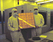
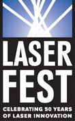
Washington, DC -- Since the laser was first demonstrated in 1960, it has found innumerable applications in science, industry, consumer products, and medicine. To commemorate the 50th anniversary of the development of the laser, the American Physical Society (APS), in partnership with the Optical Society of America (OSA), SPIE-The International Society for Optical Engineering, and the Institute of Electrical and Electronics Engineers (IEEE)-Photonics, is spearheading a year-long celebration of this historic event, described in their informative website LaserFest. To highlight 50 years of innovations in lasers and laser applications, the website presents a Timeline of Laser History Milestones. Anvik Corporation is proud to note that among the key milestones in this Timeline is the invention and demonstration of excimer laser lithography in 1982 by the Company's president, Dr. Kanti Jain.
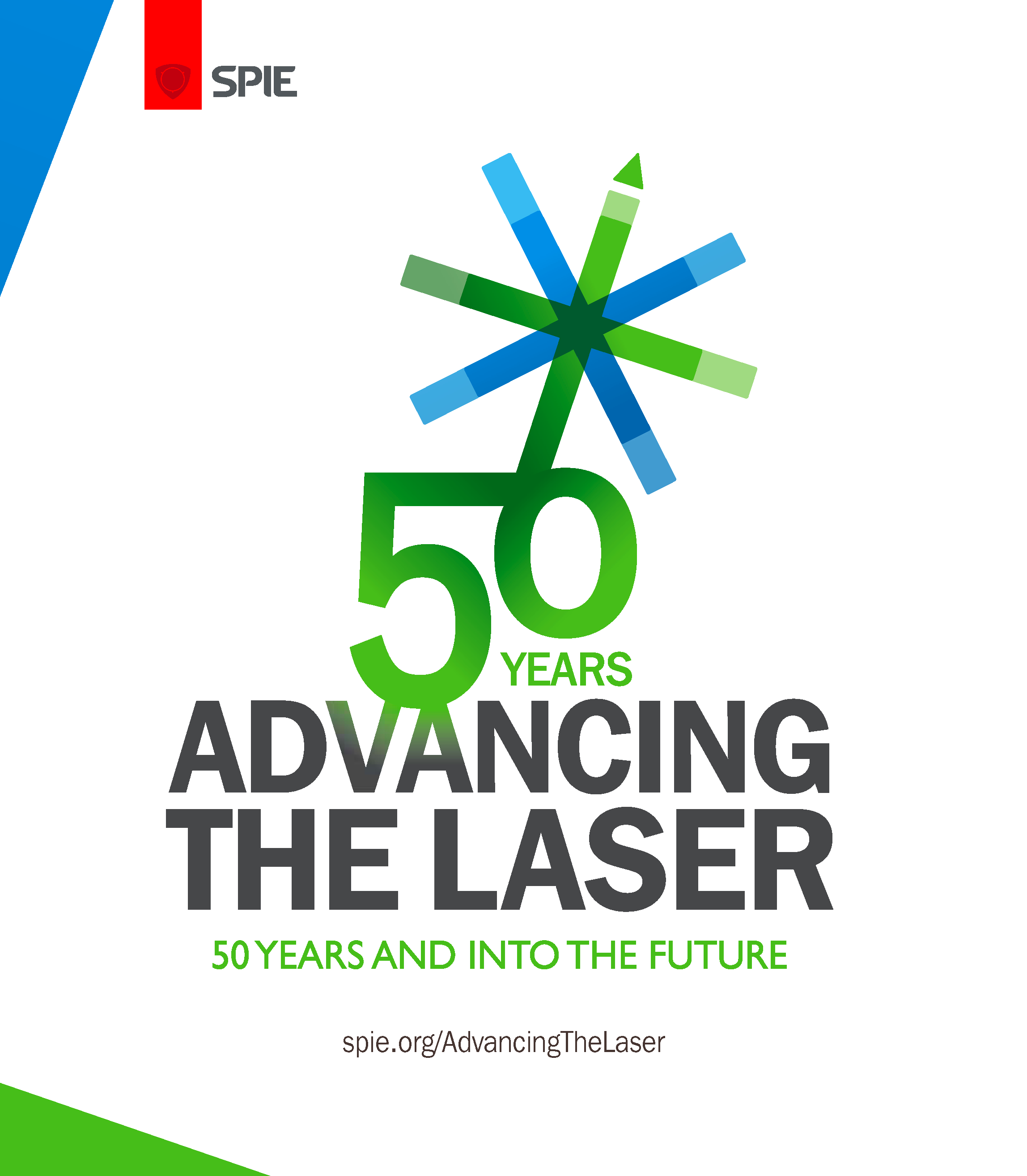
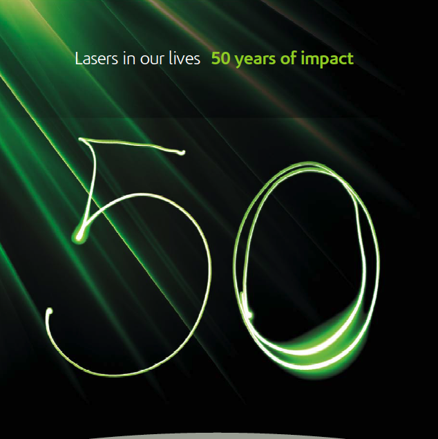
Developed by Dr. Jain at the I.B.M. San Jose Research Laboratory (now the I.B.M. Almaden Research Center), excimer laser lithography is now the predominant lithography technology used worldwide in the fabrication of microchips (integrated circuits) for the computer and electronics industry, totaling $400 billion in annual production. SPIE has featured his pioneering work in their tribute Advancing the Laser: 50 Years and Into the Future. The Engineering and Physical Sciences Research Council (EPSRC) of U.K., in their commemorative document Lasers in Our Lives: 50 Years of Impact, has also included excimer laser lithography in their 50 Years of Lasers Timeline. For his pioneering work, among the many honors Dr. Jain has received are Outstanding Innovation Awards from I.B.M., the David Richardson Medal from OSA, and election to the U.S. National Academy of Engineering (NAE).
|
February 2009
Anvik president Kanti Jain elected to the U.S. National Academy of Engineering

|
|
Washington, DC -- Dr. Kanti Jain, president of Anvik Corporation and professor of Electrical and Computer Engineering at the University of Illinois at Urbana-Champaign, has been elected to the U.S. National Academy of Engineering (NAE). Election to the NAE is among the highest professional distinctions in engineering. NAE was established in 1964 under a charter from the National Academy of Sciences as a parallel organization of outstanding engineers.
Dr. Jain is specifically honored "For contributions to the development of high-resolution, deep-ultraviolet excimer lithography for microelectronic fabrication." Excimer laser lithography systems are now used worldwide for semiconductor integrated circuit manufacturing. Dr. Ilesanmi Adesida, dean of the College of Engineering at the University of Illinois at Urbana-Champaign, explained, "Professor Kanti Jain's contributions are fundamental to how semiconductor devices and chips are manufactured today. His work has broad impact on computers, cell phones, and many modern day tools and conveniences. It is fitting that he is being elected into the Academy for his achievements." In addition, at Anvik Corporation, Dr. Jain and his team developed the technologies for large-area lithography that are widely used today in the production of flat-panel displays and televisions.
|
June 24, 2008
Anvik Corporation awarded its 60th patent
HIGH-BRIGHTNESS, COMPACT ILLUMINATOR WITH INTEGRATED OPTICAL ELEMENTS

|
|
Hawthorne, NY -- Anvik Corporation has been awarded its 60th patent. Issued on June 24, 2008 to inventor Kanti Jain, U.S. Pat. 7,390,116 describes advances made by Anvik in light sources and illumination systems for optical projection, and specifically relates to such applications in which it is important to maximize the light collection from a source lamp, to minimize the size and power requirement of the lamp, to make the spatial uniformity of the lamp's light beam high, and to collect the light within a specified numerical aperture so as to optimize the imaging performance of the projection system. An attractive application of the invention is in electronic digital projectors. This patent further strengthens Anvik's intellectual property portfolio in optical imaging and microelectronics manufacturing technologies, which now includes 68 patents, of which 61 have been issued or allowed and 7 are pending. Anvik's business in microelectronics manufacturing systems is based on its diverse patent portfolio that comprises major innovations in optical system designs, microlithography processes and tools, opto-mechanical devices, energy-efficiency technologies, and laser materials processing systems.
|
April 29, 2008
Anvik files patent infringement lawsuits against flat-panel display and television manufacturers Toshiba, Matsushita, Hitachi, and IPS Alpha
Hawthorne, NY -- Anvik Corporation has filed lawsuits against several additional major manufacturers of flat-panel displays and televisions in Japan and their U.S. subsidiaries, including Toshiba Corporation, Matsushita Electric Industrial Co., Ltd., Hitachi, Ltd., and IPS Alpha Technology, Ltd., for infringement of five Anvik patents that cover inventions in high-performance microlithography systems. Such systems are critical tools for manufacturing of microelectronics products, including flat-panel displays, televisions, semiconductor integrated circuits, and microelectronic packaging devices. The lawsuits were filed April 29, 2008 in the U.S. District Court for the Southern District of New York, White Plains Division.
The present lawsuits follow the complaints Anvik filed on February 2, 2007 against Samsung Electronics Co. Ltd. (Korea), Sharp Corporation (Japan), LG.Philips LCD Co., Ltd. (Korea), Chi Mei Optoelectronics (Taiwan), AU Optronics Corporation (Taiwan), Chunghwa Picture Tubes, Ltd. (Taiwan), Tatung Company (Taiwan), HannStar Display Corporation (Taiwan), Innolux Display Corporation (Taiwan), and AFPD PTE Ltd. (Singapore).
The inventions described and claimed in the patents are incorporated in Anvik's own microlithography systems that enable cost-effective, high-volume manufacture of a wide array of microelectronic and display products.
Anvik, based in Hawthorne, New York, is a producer of advanced microlithography and photoablation systems for high-throughput manufacturing of microelectronic devices, flat-panel displays, and flexible electronics. Anvik has advanced the state of the art of microlithography and materials processing systems for microelectronics manufacturing, and has made and installed such equipment in the U.S. and abroad.
In these lawsuits, Anvik is represented by the law firms of Bernstein Litowitz Berger & Grossman, LLP and Cozen O'Connor.
March 2008
Anvik president Kanti Jain awarded David Richardson Medal of Optical Society of America

|
|
Washington, DC -- Dr. Kanti Jain, president of Anvik Corporation, has been awarded the David Richardson Medal by the Board of Directors of the Optical Society of America for achievements in the field of optical engineering. Each year OSA presents the award to one individual chosen for his "dedication, ingenuity, and perseverance in attaining the highest level of scientific achievement in their chosen fields." The award recognizes those who have had significant influence primarily in the commercial and industrial sector of optical engineering. Dr. Jain is specifically honored for his "pioneering contributions to the development of high-resolution optical microlithography technologies, especially for the invention and development of excimer laser lithography technologies and systems for production of microelectronic devices," according to the OSA citation. Excimer laser lithography systems are now used worldwide for semiconductor integrated circuit manufacturing. In addition, at Anvik, Dr. Jain and his team developed the technologies for large-area lithography that are widely used today in the production of flat-panel displays and televisions.
Optical Society of America Press Release
|
February 2, 2007
Anvik files patent infringement lawsuits against Samsung, Sharp, LG.Philips, CMO, AUO, CPT, Toppan, and other flat-panel display and television manufacturers
Hawthorne, NY -- Anvik Corporation has filed lawsuits against several major manufacturers of flat-panel displays and televisions and their U.S. subsidiaries, including Samsung Electronics Co. Ltd. (Korea), Sharp Corporation (Japan), LG.Philips LCD Co., Ltd. (Korea), Chi Mei Optoelectronics (Taiwan), AU Optronics Corporation (Taiwan), Chunghwa Picture Tubes, Ltd. (Taiwan), Tatung Company (Taiwan), Toppan Printing Co., Ltd. (Japan), HannStar Display Corporation (Taiwan), Innolux Display Corporation (Taiwan), and AFPD PTE Ltd. (Singapore), for infringement of five Anvik patents that cover inventions in high-performance microlithography systems. Such systems are critical tools for manufacturing of microelectronics products, including flat-panel displays, televisions, semiconductor integrated circuits, and microelectronic packaging devices. The lawsuits were filed February 2, 2007 in the U.S. District Court for the Southern District of New York, White Plains Division.
The inventions described and claimed in the patents are incorporated in Anvik's own microlithography systems that enable cost-effective, high-volume manufacture of a wide array of microelectronic and display products.
Anvik, based in Hawthorne, New York, is a producer of advanced microlithography and photoablation systems for high-throughput manufacturing of microelectronic devices, flat-panel displays, and flexible electronics. Anvik has advanced the state of the art of microlithography and materials processing systems for microelectronics manufacturing, and has made and installed such equipment in the U.S. and abroad.
In these lawsuits, Anvik is represented by the law firms of Bernstein Litowitz Berger & Grossman, LLP and Cozen O'Connor.
February 2006
Anvik president Kanti Jain elected Fellow of IEEE

|
|
Washington, DC -- Dr. Kanti Jain, president of Anvik Corporation, has been conferred the title of IEEE Fellow by the Board of Directors of the Institute of Electrical and Electronics Engineers for his work on high-resolution excimer laser lithography. As presented in an IEEE press release: "An important part of the IEEE's mission is to recognize the professional achievements of its members. The Institute's highest honor is the rank of IEEE Fellow, bestowed on members who have contributed 'to the advancement or application of engineering science and technology'." The technology of excimer laser lithography was invented and developed by Dr. Jain at IBM in the 1980's and is now used worldwide in semiconductor chip production.
|
January 2006
University of Illinois at Urbana-Champaign appoints Anvik president Kanti Jain Professor of Electrical and Computer Engineering
Urbana, IL -- Dr. Kanti Jain, president of Anvik Corporation, has been appointed Professor of Electrical and Computer Engineering at the University of Illinois at Urbana-Champaign. At Illinois, his objective is to initiate a number of new research programs that will advance the state-of-the-art in microelectronic, optoelectronic, microsystem and biophotonic devices by developing and exploiting novel micro/nano-fabrication technologies. These fabrication technologies will enable patterning and microstructuring of a variety of organic and inorganic materials -- including new polymers, semiconductors, metals, dielectrics and biological materials -- and producing structures, devices and systems previously not deemed possible. Dr. Jain will continue in his responsibility as president of Anvik Corporation.
October 5, 2005
Anvik files patent infringement lawsuit against Nikon
Hawthorne, NY -- Anvik Corporation has filed a lawsuit against Nikon Corporation and two of its U.S. subsidiaries for infringement of six Anvik patents that cover inventions in high-performance microlithography systems. Such systems are critical tools for manufacturing of microelectronics products, including semiconductor integrated circuits, microelectronic packaging devices, and flat-panel displays. The lawsuit was filed September 9, 2005 in the U.S. District Court for the Southern District of New York, White Plains Division. Named defendants are Nikon Precision, Inc., Nikon Research Corporation of America, and Nikon Corporation.
The inventions described and claimed in the patents are incorporated in Anvik's own microlithography systems that enable cost-effective, high-volume manufacture of a wide array of microelectronic and display products.
Anvik, based in Hawthorne, New York, is a producer of advanced microlithography and photoablation systems for high-throughput manufacturing of microelectronic devices, flat-panel displays, and flexible electronics. Anvik has advanced the state of the art of microlithography and materials processing systems for microelectronics manufacturing, and has made and installed such equipment in the U.S. and abroad.
In these lawsuits, Anvik is represented by the law firms of Bernstein Litowitz Berger & Grossman, LLP and Cozen O'Connor.
March 22, 2005
Anvik Corporation awarded its 50th patent
MASKLESS LITHOGRAPHY WITH MULTIPLEXED SPATIAL LIGHT MODULATORS
|
|
|
Hawthorne, NY -- Anvik Corporation has been awarded its 50th patent. Issued on March 22, 2005 to inventor Kanti Jain, U.S. Pat. 6,870,554 describes recent advances made by Anvik in maskless lithography technology, especially directed toward high-throughput fabrication of sub-100 nm microelectronic devices. This patent further strengthens Anvik's intellectual property portfolio in micro- and nanolithography technology, which now includes 40 patents, of which 7 are in maskless lithography. Anvik's business in microelectronics manufacturing systems is based on a diverse patent portfolio that comprises major innovations in optical system designs, microlithography processes and tools, opto-mechanical devices, energy-efficiency technologies, and laser materials processing systems.
|
|